 中文
中文  English
 Product Center
Products



Product Features
High photoelectric conversion efficiency and stability Low "wavelength-temperature" sensitivity
2. Low thermal resistance and high reliability
3. Other bands and sizes can be provided as required
Application fields
Used in machine vision, consumer electronics, infrared lighting, industrial scenes and other fields.
Gallium arsenide (GaAs) is a kind of semiconductor material with excellent performance, which has the characteristics of direct band gap, high electron mobility, high frequency and low noise, high conversion efficiency and so on. It is widely used in optoelectronics and microelectronics industry. In the application level of optoelectronic industry, gallium arsenide single product can be used to make LED (light emitting diode), LD (laser), photovoltaic devices, etc. In the application level of microelectronics industry, it can be used to make MESFET (metal semiconductor field effect transistor), HEMT (high electron mobility transistor), IBT (heterojunction bipolar transistor), IC, microwave diode, Hal1 device, etc.
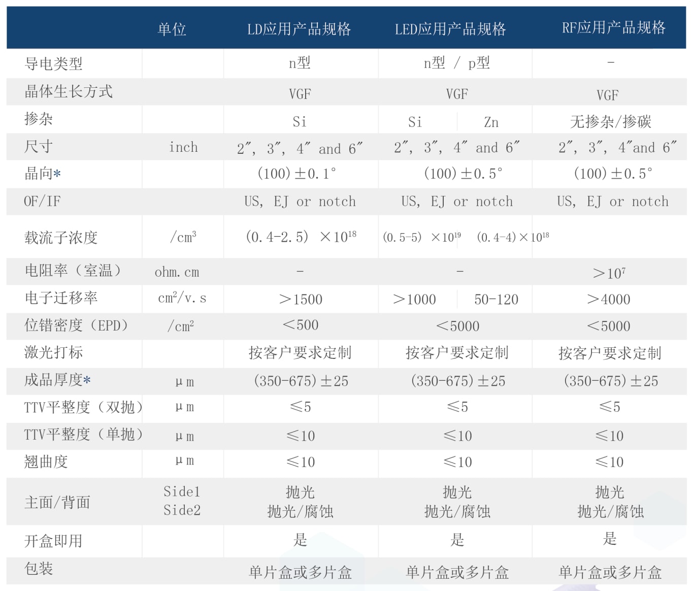
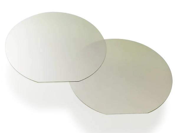
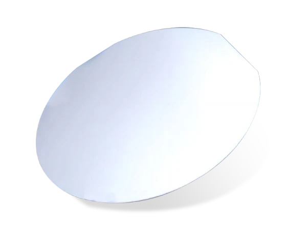
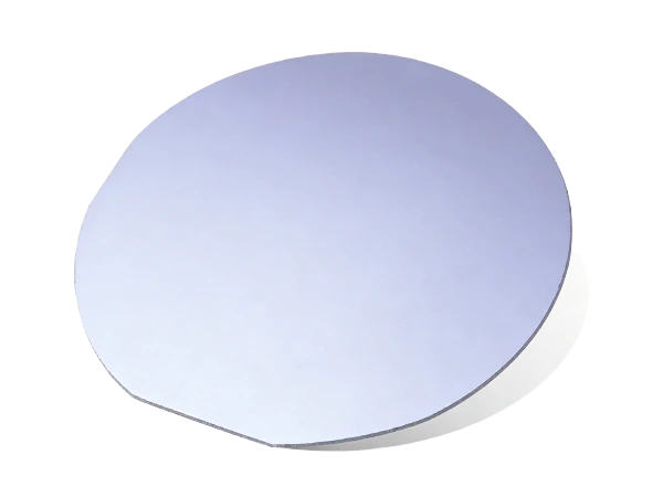
Weixin Optoelectronics offers 2-6 inch GaAs substrates grown using VGF technology, including semi-insulating GaAs substrates (undoped) and semiconducting GaAs substrates (Si-or Zn-doped), as well as low-dislocation GaAs substrates for VCSEL and RF applications. Can also be customized according to customer needs, non-standard thickness and crystal direction of GaAs substrate.