 中文
中文  English
 Product Center
Products



Product Features
High photoelectric conversion efficiency and stability Low "wavelength-temperature" sensitivity
2. Low thermal resistance and high reliability
3. Other bands and sizes can be provided as required
Application fields
Used in machine vision, consumer electronics, infrared lighting, industrial scenes and other fields.
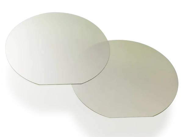
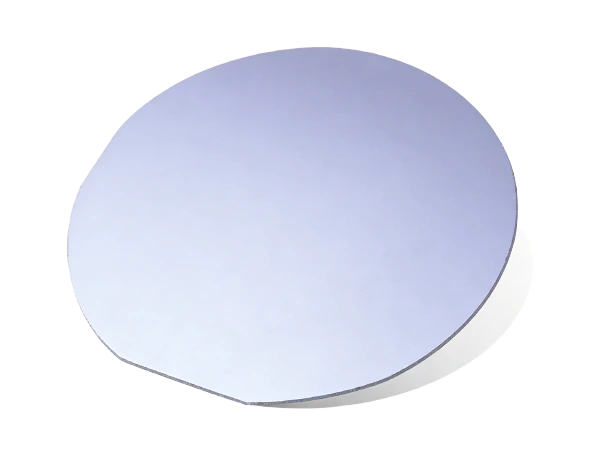
Indium phosphide (InP), as a kind of excellent semiconductor material, has the advantages of high electron mobility, good radiation resistance and large band gap. It is mainly used in the field of communication and microelectronics, including optical fiber communication, wireless network, mobile phone, Bluetooth communication, satellite communication, satellite communication microwave field, and radio frequency integrated circuit.
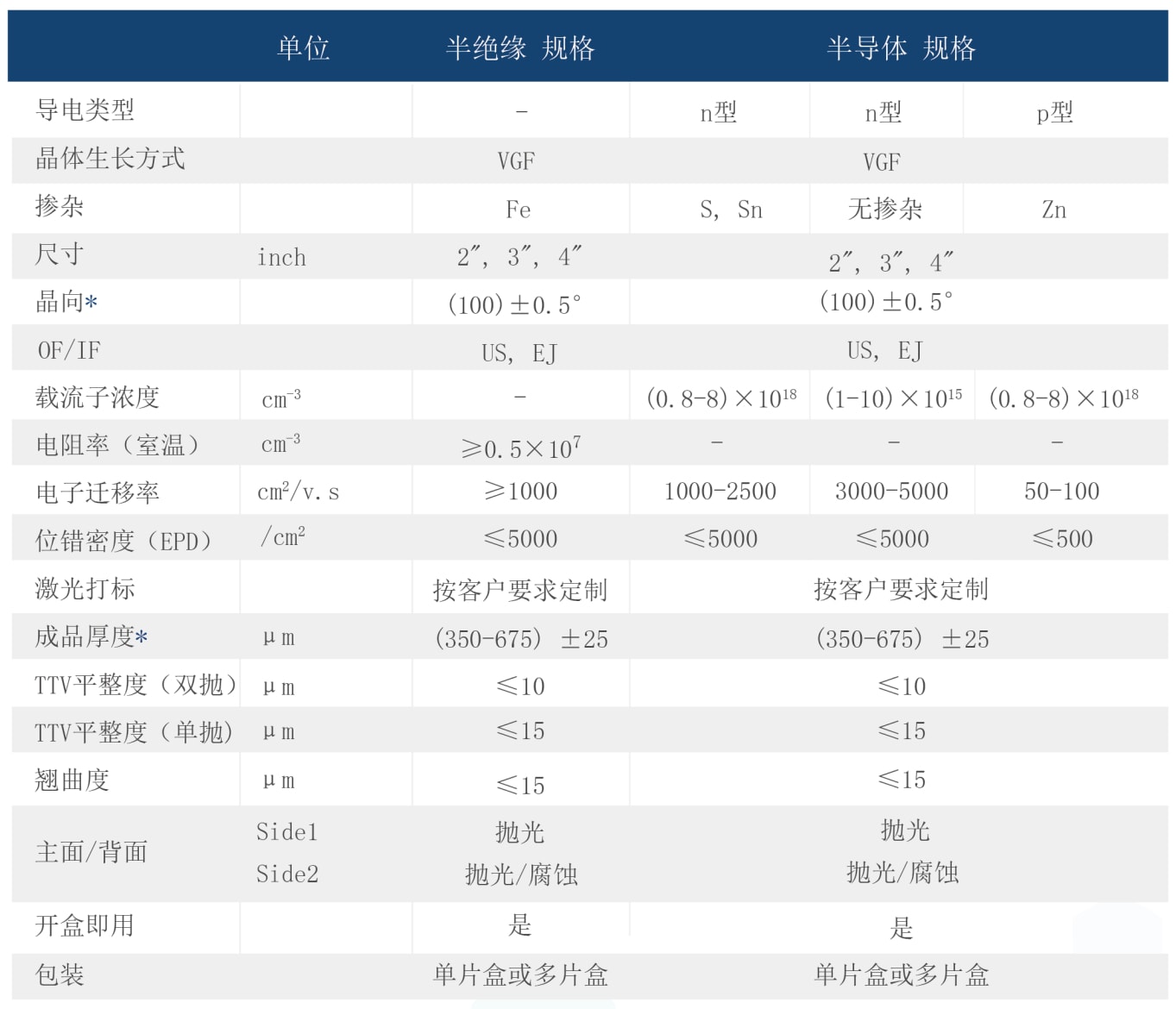
Weixin Optoelectronics can provide InP substrates using 2-4 inches, including semi-insulating InP substrates (Fe-doped) and semiconductor InP substrates (Si-doped or Zn-doped), as well as low-dislocation InP substrates for specific applications. Can also be customized according to customer needs, non-standard thickness and crystal direction of InP substrate.