 中文
中文  English
 Product Center
Products



Product Features
High photoelectric conversion efficiency and stability Low "wavelength-temperature" sensitivity
2. Low thermal resistance and high reliability
3. Other bands and sizes can be provided as required
Application fields
Used in machine vision, consumer electronics, infrared lighting, industrial scenes and other fields.
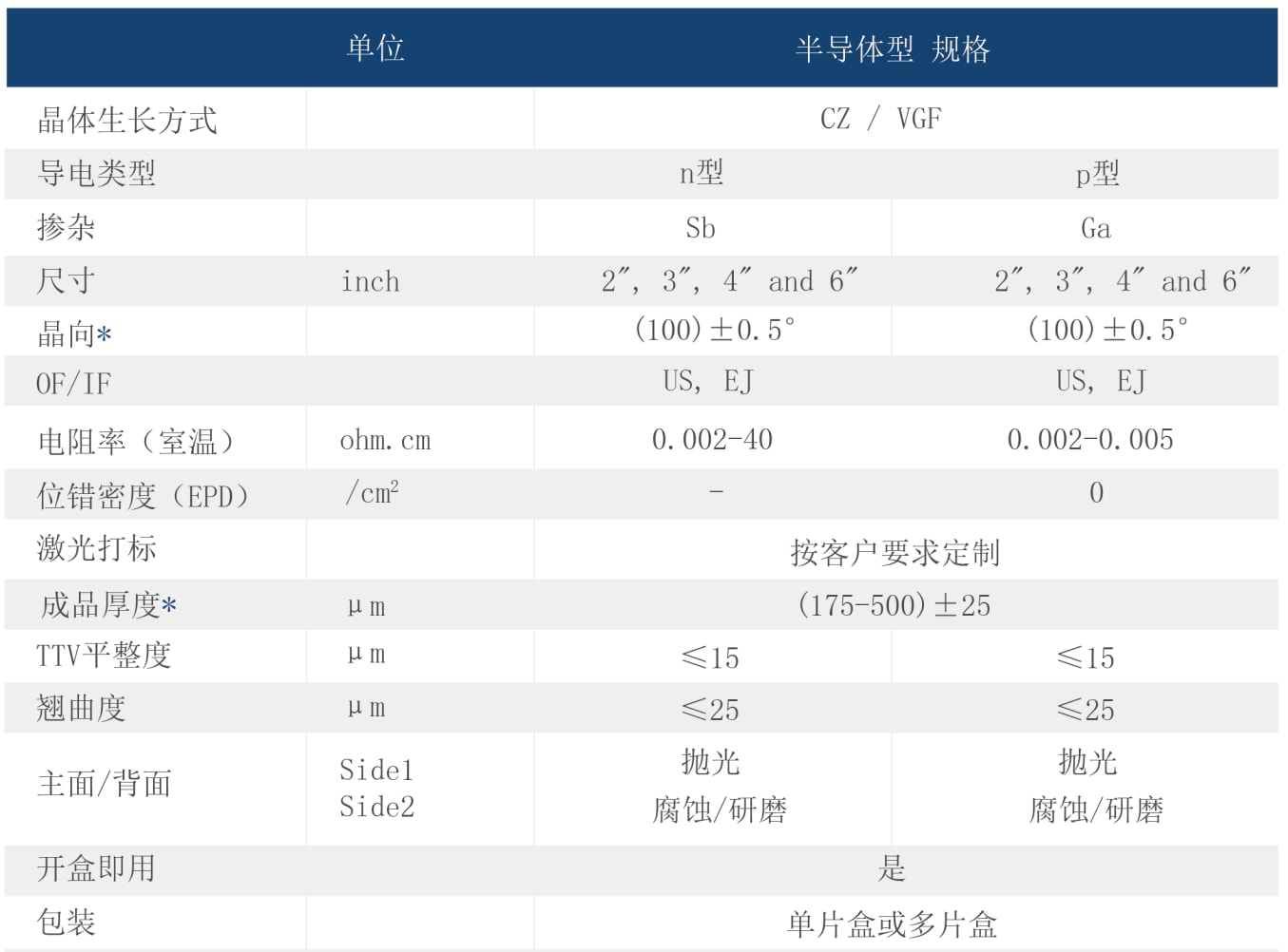
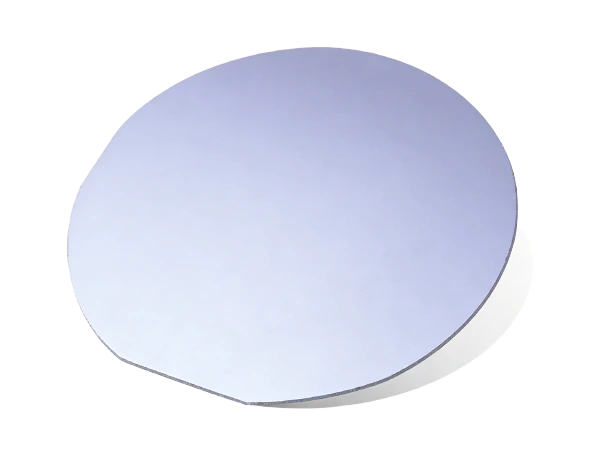
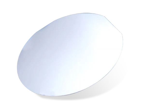
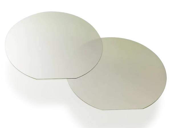
Germanium monocrystalline wafer is an important semiconductor substrate material, which has good semiconductor properties, such as electron mobility, hole mobility and so on. Mainly used for ground concentrated photovoltaic power plants (CPV), space solar panels and ultra-high brightness LED substrate materials.
Weixin Optoelectronics can provide low dislocation or zero dislocation substrates with specifications including 2 inches, 3 inches, 4 inches and 6 inches. Ge substrates with non-standard thickness and crystal direction can also be customized according to customer requirements.